larger largest
Table of Contents | Index | Previous Section | Next Section
|
|
|
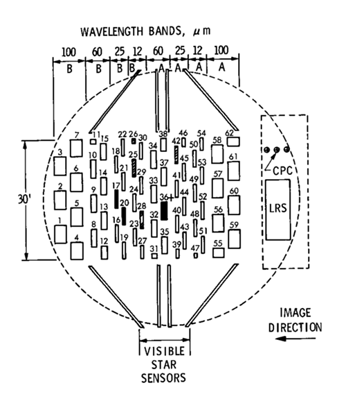
Figure II.C.6 A schematic drawing of the IRAS focal plane. The numbered
rectangles in the central portion each represent the field of view of a
detector, filter, and field lens combination. The image of a source
crossed the focal plane in the Y direction as indicated. The filled-in
detectors were inoperative while the cross-hatched detectors showed
degraded performance during the mission.
larger largest |
The focal plane assembly contained the infrared and visible detectors, cold electronics, and associated masks, filters and field optics. It consisted of 62 infrared channels and eight visible channels. The infrared channels were divided into eight modules, two for each color band with each module containing either seven or eight detectors. Figure II.C.6 shows the layout of the focal plane and the numbers assigned to individual infrared detectors. Table II.C.3 lists the positions of the center of each detector mask relative to the boresight and the size of each mask projected through the optical system onto the sky. The detector masks were rectangular in aspect and infrared sources scanned across the focal plane parallel to the narrow dimension of the detectors in all observational modes.
| Det | Offset Step |
Nominal Gain1 |
Mask Location arc min |
Size arc min | ||
|---|---|---|---|---|---|---|
| No. | (0-7) | Y4 | Z5 |  Z Z |
Y |
|
| --100 µm Band, Module B-- | ||||||
| 1 | 3 | 26.6 | 27.87 | 8.71 | 5.05 | 3.03 |
| 2 | 3 | 24.6 | 27.80 | 0.04 | 5.05 | 3.03 |
| 3 | 3 | 25.4 | 27.86 | -8.62 | 5.05 | 3.03 |
| 4 | 4 | 24.1 | 23.83 | 12.86 | 4.68 | 3.03 |
| 5 | 32 | 26.2 | 24.04 | 4.37 | 5.05 | 3.03 |
| 6 | 4 | 25.9 | 23.65 | -4.29 | 5.05 | 3.03 |
| 7 | 3 | 24.7 | 23.78 | -12.77 | 5.05 | 3.03 |
| --60 µm Band, Module B-- | ||||||
| 8 | 3 | 21.2 | 19.64 | 9.80 | 4.75 | 1.51 |
| 9 | 3 | 20.2 | 19.72 | 1.14 | 4.75 | 1.51 |
| 10 | 4 | 21.3 | 19.74 | -7.53 | 4.75 | 1.51 |
| 11 | 3 | 21.1 | 19.70 | -14.46 | 1.30 | 1.51 |
| 12 | 3 | 21.3 | 17.20 | 13.49 | 3.45 | 1.51 |
| 13 | 3 | 23.1 | 17.19 | 5.47 | 4.75 | 1.51 |
| 14 | 3 | 21.0 | 17.20 | -3.20 | 4.75 | 1.51 |
| 15 | 4 | 21.3 | 17.20 | -11.86 | 4.75 | 1.51 |
| --25 µm Band, Module B-- | ||||||
| 16 | 4 | 12.3 | 14.01 | 8.71 | 4.65 | 0.76 |
| 173 | 3 | 11.8 | 14.04 | 0.04 | 4.65 | 0.76 |
| 18 | 4 | 11.3 | 14.04 | -8.62 | 4.65 | 0.76 |
| 19 | 4 | 13.1 | 12.24 | 12.96 | 4.48 | 0.76 |
| 203 | 4 | 11.7 | 12.27 | 4.37 | 4.65 | 0.76 |
| 21 | 4 | 11.8 | 12.26 | -4.29 | 4.65 | 0.76 |
| 22 | 4 | 11.9 | 12.27 | -12.88 | 4.48 | 0.76 |
| --12 µm Band, Module B | ||||||
| 23 | 4 | 14.2 | 9.47 | 9.81 | 4.45 | 0.76 |
| 24 | 4 | 14.8 | 9.46 | 1.14 | 4.45 | 0.76 |
| 25 | 4 | 15.5 | 9.47 | -7.52 | 4.45 | 0.76 |
| 26 | 3 | 14.3 | 9.48 | -14.50 | 1.20 | 0.76 |
| 27 | 4 | 14.2 | 7.71 | 13.55 | 3.33 | 0.76 |
| 28 | 3 | 15.3 | 7.71 | 5.47 | 4.55 | 0.76 |
| 29 | 4 | 13.9 | 7.70 | -3.19 | 4.55 | 0.76 |
| 30 | 4 | 14.5 | 7.71 | -11.86 | 4.55 | 0.76 |
| --60 µm Band, Module A-- | ||||||
| 31 | 3 | 20.8 | 4.56 | 14.55 | 1.28 | 1.51 |
| 32 | 3 | 20.8 | 4.59 | 7.61 | 4.75 | 1.51 |
| 33 | 3 | 22.6 | 4.58 | -1.06 | 4.75 | 1.51 |
| 34 | 3 | 20.8 | 4.59 | -9.73 | 4.75 | 1.51 |
| 35 | 3 | 21.0 | 2.06 | 11.94 | 4.75 | 1.51 |
| 363 | 3 | 20.7 | 2.06 | 3.27 | 4.75 | 1.51 |
| 37 | 4 | 20.8 | 2.11 | -5.40 | 4.75 | 1.51 |
| 38 | 3 | 18.9 | 2.10 | -13.41 | 3.47 | 1.51 |
| --25 µm Band, Module A-- | ||||||
| 39 | 4 | 15.2 | -1.16 | 14.05 | 2.33 | 0.76 |
| 40 | 4 | 15.7 | -1.16 | 6.55 | 4.65 | 0.76 |
| 41 | 3 | 14.7 | -1.16 | -2.12 | 4.65 | 0.76 |
| 42 | 4 | 16.1 | -1.14 | -10.78 | 4.65 | 0.76 |
| 43 | 3 | 13.9 | -2.92 | 10.88 | 4.65 | 0.76 |
| 44 | 4 | 14.8 | -2.92 | 2.22 | 4.65 | 0.76 |
| 45 | 3 | 15.3 | -2.93 | -6.45 | 4.65 | 0.76 |
| 46 | 3 | 15.4 | -2.92 | -13.95 | 2.33 | 0.76 |
| --12 µm Band, Module A-- | ||||||
| 47 | 4 | 14.5 | -5.67 | 14.64 | 1.18 | 0.76 |
| 48 | 3 | 14.0 | -5.67 | 7.65 | 4.55 | 0.76 |
| 49 | 4 | 14.4 | -5.67 | -1.02 | 4.55 | 0.76 |
| 50 | 2 | 14.1 | -5.66 | -9.68 | 4.55 | 0.76 |
| 51 | 3 | 14.2 | -7.42 | 11.98 | 4.55 | 0.76 |
| 52 | 3 | 14.3 | -7.43 | 3.32 | 4.55 | 0.76 |
| 53 | 4 | 14.4 | -7.43 | -5.35 | 4.55 | 0.76 |
| 54 | 4 | 13.8 | -7.42 | -13.41 | 3.36 | 0.76 |
| --100 µm Band, Module A-- | ||||||
| 55 | 4 | 22.9 | -11.33 | 13.95 | 2.52 | 3.03 |
| 56 | 4 | 27.3 | -11.42 | 6.55 | 5.05 | 3.03 |
| 57 | 3 | 26.2 | -11.51 | -2.12 | 5.05 | 3.03 |
| 58 | 4 | 27.6 | -11.41 | -10.79 | 5.05 | 3.03 |
| 59 | 3 | 26.8 | -15.34 | 10.88 | 5.05 | 3.03 |
| 60 | 3 | 26.9 | -15.49 | 2.21 | 5.05 | 3.03 |
| 61 | 4 | 26.8 | -15.40 | -6.46 | 5.05 | 3.03 |
| 62 | 4 | 26.5 | -15.38 | -13.85 | 2.53 | 3.03 |
| (1) | The ratios of nominal to low gain and nominal to high gain
are 7.18, 0.107; 5.98, 0.109; 10.8, 0.102; and 13.4, 0.100 for the 12, 25, 60, and 100 µm channels. |
|||||
| (2) | Offset step changed after launch to 2 | |||||
| (3) | Channel inoperative during mission | |||||
| (4) | During survey scans sources move from -Y to +Y | |||||
| (5) | Negative Z corresponds to larger angle to the Sun ( ) ) |
|||||
|
|
|
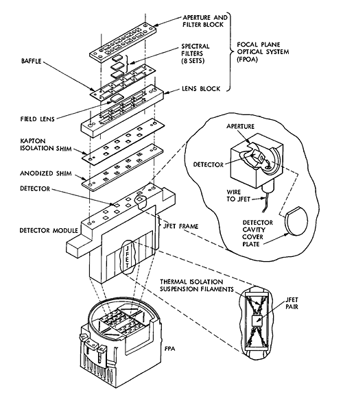
Figure II.C.7 Infrared subarray module exploded view showing module components.
larger largest |
Figure II.C.7 shows an exploded view of the
focal plane. Infrared radiation passed through the field mask and spectral
filters and was focused by the field lens onto the aperture defining the
detector cavity entrance. The detector cavities were constructed of Au:Pt
alloy to provide local high-Z shielding to absorb  -rays
with energies less than about 100 keV. In addition, for the 60 and 100
µm detectors, the cavities were designed as reflecting integrating
cavities to increase photon absorption in the Ge:Ga material.
-rays
with energies less than about 100 keV. In addition, for the 60 and 100
µm detectors, the cavities were designed as reflecting integrating
cavities to increase photon absorption in the Ge:Ga material.
The visible wavelength channels were similar to the infrared wavelength channels in construction, except that they used visible light filters, no field lens, and silicon diode detectors. The visible wavelength detectors were placed in a double"V" arrangement in order to provide two-axis spacecraft attitude information during star crossings.
|
|
|
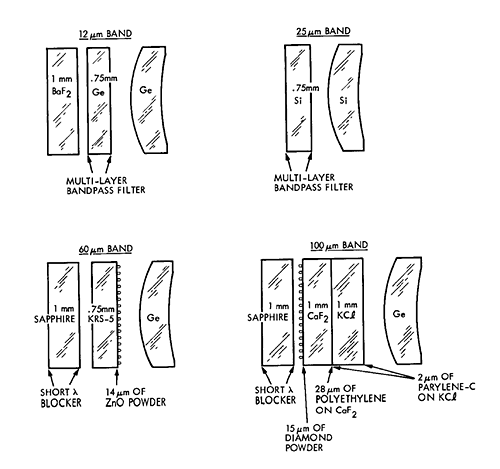
Figure II.C.8 Focal plane array filter and lens components and
configuration.
larger largest |
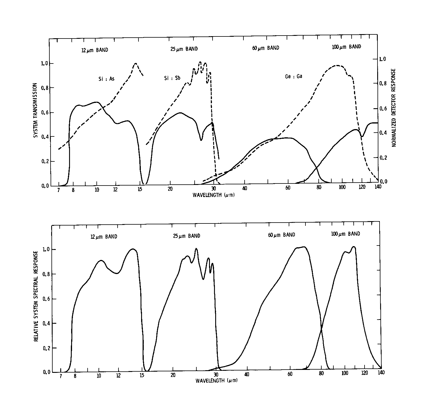
Figure II.C.8 shows the focal plane filter/lens combinations and configurations for each color band and Table II.C.4 summarizes the optical characteristics of the survey array. The detailed optical system transmission, detector spectral response and overall relative spectral response for the four infrared bands are shown in Figs. II.C.9.a,b and are listed in Table II.C.5. These parameters were determined from pre-flight measurements of sample filters, field lens material and, with the exception of the 100 µm detectors, spare flight detectors. The response of the Ge:Ga detectors used at 100 µm was assumed to be the same as that of the 60 µm detectors even though the material came from a different source. Additional details of the focal plane optics can be found in Bamberg and Zuan (1984) and Darnell (1984).
|
|
|
Figure II.C.9 a) Response vs. wavelength of optical components. Solid
lines show the transmission of filters and lenses. Dashed lines show
relative detector response to constant energy input; b) Relative system
spectral response.
larger largest |
| BAND | 12 µm | 25 µm | 60 µm | 100 µm |
|---|---|---|---|---|
| FILTER FUNCTIONS | ||||
| Short Wavelength Blocking |
MLIF* | MLIF | MLIF + Sapphire + ZnO powder |
MLIF + Sapphire + CaF(-2)+ KCL + Diamond powder |
| Short Wavelenght Cuton |
MLIF | MLIF | Sapphire + MLIF |
KCL |
| Long Wavelength Cutoff |
MLIF | Si:Sb | KRS-5 | Ge:Ga |
| Long Wavelength Blocking |
BaF(-2)+ MLIF+ Si:As |
Si:Sb | KRS-5 | Ge:Ga |
| FIELD LENS | ||||
| Materials | Ge | Si | Ge | Ge |
| Anti-reflection coating |
MLIF | MLIF |  /4 /4parylene-C |
/4 parylene-C |
| Focal length | 6.53 mm | 6.59 mm | 6.98 mm | 8.34 mm |
| Exit pupil diameter | 1.0 mm | 1.0 mm | 1.0 mm | 1.16 mm |
| DETECTORS | ||||
| Materials | Si:As | Si:Sb | Ge:Ga | Ge:Ga |
| size(LxW), mm | 1.0 × 1.78 | 1.0 × 1.78 | 1.5 × 1.5 | 1.25 × 1.25 |
| Electrode Spacing (mm) | 0.64 | 0.71 | 1.0 | 1.25 |
| OPTICAL PERFORMANCE | ||||
| Bandwidth (FWHM) | 7.0 µm | 11.15 µm | 32.5 µm | 31.5 µm |
| Average Inband Transmission | 0.54 | 0.50 | 0.29 | 0.34 |
| OUT-OF-BAND LEAKS | ||||
| ShortWavelength | <2 × 10⁻⁵ | <5 × 10⁻⁵ | <2 × 10⁻⁴** | <9 × 10⁻²** |
| Long Wavelength | <3 × 10⁻⁶ | <2 × 10⁻⁴ | <2 × 10⁻⁴ | <5 × 10⁻² |
| *MLIF = multi-layer interference filter **See Section II.C.4 |
||||
Out-of-band leaks listed in Table II.C.4 are defined
as the ratio of the integrated energy longward or shortward of the 2% relative
response wavelength to the integrated inband energy. The calculations were
based on illumination from a 2000 K blackbody for short wavelength leaks
and a 200 K blackbody for long wavelength leaks. The tabulated limits come
from tests of the final flight focal plane except for the 100 µm
detectors which were changed shortly before launch. These measured limits
differ from an earlier set of measurements of the individual components
At 100 µm these latter tests give an out-of-band rejection
less than 1.5 × 10⁻³ for a 2000 K source, significantly lower than the
upper limit in the table. At 60 µm these component tests indicated
the presence of a spectral leak between 1.6 and 7 µm that could
be as large as 0.02 for a 2000 K source and 0.08 for a 10,000 K source,
significantly larger than the tabulated limit. The origin of the discrepancy
is not understood. A discussion of the in-flight tests of the spectral
response is given in Section IV.B.2, and
of the possible impact of leaks on the calibration in VI.C.
Table of Contents | Index | Previous Section | Next Section
