The
TopHat detectors are monolithic silicon bolometers.
These devices measure the intensity of radiation by
absorbing it and converting it to a temperature rise
in the absorber material. An embedded semiconductor
device (thermistor) converts this temperature rise into
a change in resistance, which can then be measured electrically.
Bolometers
are the most sensitive detectors for broadband low-background
radiation. With these detectors mounted in a 3He cryostat,
TopHat will be able to make observations of cosmic microwave
background anisotropy of unprecedented sensitivity,
in spite of the relatively short integration time available
with a balloon-borne telescope.
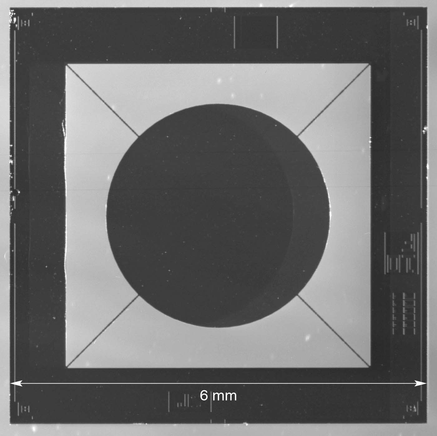
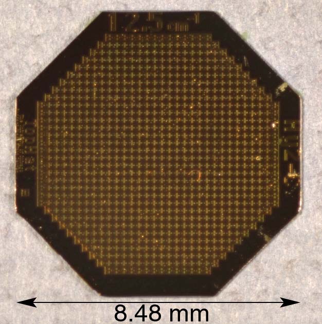
Our
bolometers are micromachined from silicon in Goddard's
Device Development Laboratory (DDL). The central disk
is coated with a layer of bismuth which absorbs the
incident radiation. The disk, which is only 5 microns
thick, has a very low heat capacity, so even small amounts
of radiation result in a significant temperature increase.
Figure
1.
This
figure shows
an actual TopHat detector. The thin supporting legs
are 10 microns wide by 5 microns thick.
The
temperature of the disk is measured by a thermistor,
which is formed by doping the silicon by ion implantation.
The disk is suspended from the frame by four thin legs.
The legs give a low thermal conductivity path between
the disk and the frame. The noise in these detectors
due to Johnson noise and phonon noise is kept low by
operating them at low temperature; for TopHat, this
is 240 mK (or -273.5 C, just 0.24 C warmer than absolute
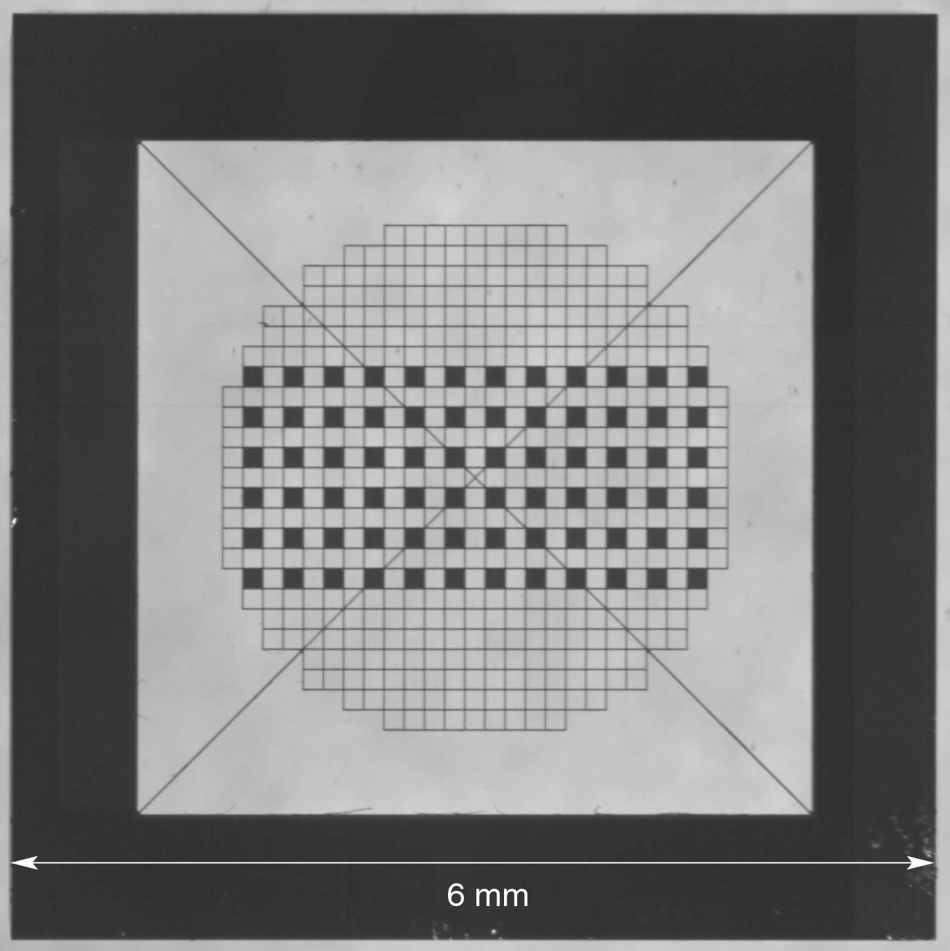
zero temperature). We are also building perforated detectors,
which differ in that the disk, instead of being solid,
is a web of silicon. See Figure 2.
Figure
2.
These
behave just like the solid detectors because the wavelengths
we are interested in are much longer than the spacing
of the web. To the incident radiation, the detector
looks just like a solid wheel of material. These perforated
detectors are useful because the cross section of the
absorber is much smaller than the solid counterparts.
Because the sensitivity of a detector to spurious cosmic
ray events is proportional to its cross section, these
detectors are ideal for making high sensitivity measurements
in higher radiation environments such as in space, or
at high altitudes in Antarctica. This minimizes signals
from the random cosmic ray events which can increase
noise as well as saturate a bolometer by causing large
temperature excursions.
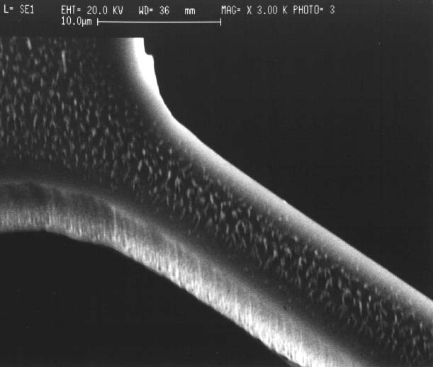
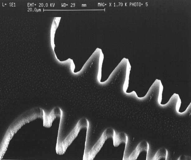
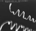
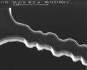
A
problem to be overcome in manufacturing bolometers by
micromachining silicon is roughening the legs. Straight,
smooth leg walls cause the legs to act as a waveguide
for phonons, resulting in a higher than acceptable thermal
conductivity. A previous method for solving this problem
has been roughening the back of the leg. This process
is difficult to control and has resulted in unreliable
strength of the legs. The Tophat detectors are pioneering
a technique of roughening the sides of the legs. This
is done by reactive ion etching (RIE) of patterned legs
with non-smooth geometries.

Figure
3.
Figure
3. shows the smooth, normal legs on a bolometer. We
can apply some mild roughness like this (Figure 4.),
or make the edges really rough like this (Figure 5.).
The optimum amount of roughness depends on the exact
design and intended use of the bolometer.
|
Figure
4.
|
Figure
5.
|
The
TopHat Band Defining Filters
Astronomical
objects can be characterized by their distinctive, and
often steep, frequency spectra. Foregrounds, such as
that due to the Earth's atmosphere, also emit strongly
frequency dependent radiation. In order to understand
the data from a detector, it is essential that we know
accurately the frequency band that it is sensitive to.
In the Tophat detector system, the in-band and near-band
shape of the passband is primarily determined by the
band defining filters. Thus it is essential that these
filters give predictable and stable performance.
The
band defining filters for Tophat are three layer filters
in a double quarterwave configuration.
Figure
6.
Each
layer is an inductive mesh metal pattern on a 0.5 um
thick silicon nitride membrane. A layer by itself acts
as a narrow bandpass filter; by stacking them as a double
quarterwave we obtain the desired width of the passband.
The spacing of the layers is set by the thickness of
the silicon wafer. A typical bandpass for these filters
is shown *here* (PostScript plot).
A
previous method of building these filters is to place
the metal pattern on a plastic substrate, such as Mylar,
and gluing them in a stack with machined metal spacers.
Using a silicon nitride membrane, which is formed on
a silicon wafer from which the spacer is later formed,
gives a substrate which is reliably flatter and therefore
gives more reliable and predictable performance.
The
metal patterns on these filters are formed using a resist
lift-off process, rather than the more traditional etch
process. In the etch process, the wafer is coated with
a sheet of metal, then with a photoresist layer which
is patterned with the desired metal pattern. An isotropic
chemical etch then removes the metal where there are
holes in the resist. The new lift-off process gives
much sharper and better defined features -- sharper
features gives better and more predictable filter response.
In this process the resist is applied to the wafer and
patterned with holes where the metal is desired. The
resist is processed in a manner that results in an overhang
at the edges. Then metal is sputtered onto the wafer.
When the resist is removed, the metal remains only where
the resist was perforated.
For
information on the TopHat Frequency Selective Bolometer
see meyer.pdf.