Main
· Science
· Instrument
· Backend
· Channelizer
· Design
· Software
· Transmission line
» Power Splitter
· Bandpass Filter
· Mixer
· Amplifier
· Jumper
· SMA Connector
· Enclosure
· Fabrication
· Performance
· Future Revisions
· Correlator
· Receiver
· Optics
· Data Acquisition
· Local Oscillator
· Base
· Analysis
· Results
· Publications
· Team
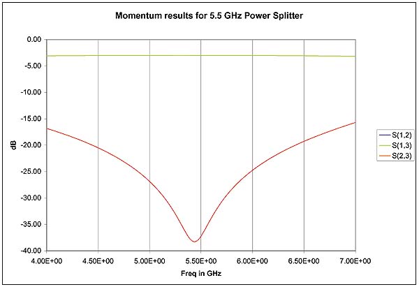
The MINT power splitters are based on the Wilkinson Power Splitter design. The Wilkinson Power splitter is a 3-port device, and it is not lossless. We use two types of filters; a narrow-band and a broadband version. The narrow-band versions are used to split the monochromatic LO signals that feed into the mixers. Since there are 2 different LO frequencies, 4.5 and 5.5 GHz, there are 2 different narrow-band power splitters. The broadband splitter is the one used to actually split the 2-6 GHz signal. As it will be seen, the narrow-band versions have just enough bandwidth to possibly be used as the broadband splitter. We felt, however, that it would be smarter to over-design to account simulation inaccuracy.
Narrow Band
The theory of operation for the narrow-band version is described in many textbooks, for example, Pozar pg 363 sec 7.3. The narrow-band version consists of a T-junction power-divider feeding two quarter-wave transformers which are connected via a resistor at the output port end. To ensure that all the ports are matched to 50 Ohms, the quarter wave sections are chosen to be 50*(2)^1/2 Ohms and the resistor is 100 Ohms. The important feature of the power divider is that the output ports are isolated, that is, input power into one of the output ports is not seen on the other output port. The disadvantage is that since there is a resistor, there device is lossy. Half of the power is lost into the resistor when it is driven at the output. The resistor also tends to limit the maximum frequencies of possible designs. Since there is a quarter-wave transformer, the bandwidth is limited.
Power splitters can have many different geometries. We chose circular sections because they are the most gentle way to bend the 1/4-wave transformers.
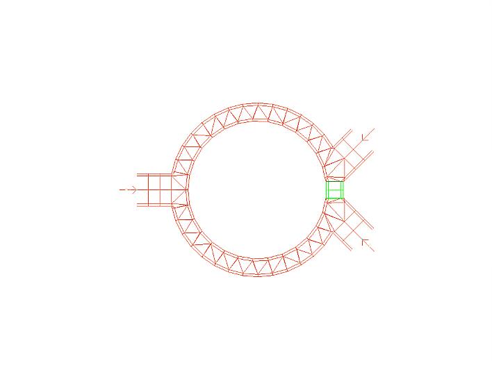
fig 1. Meshing of 4.5 GHz power splitter. For a description of the simulation process, see the filter section.
The simulation includes an attempt at simulating the thin-film resistor. It's the colored section at the right end. The resistor just consists of a conductor with a finite conductance. Of course, a real resistor is a bit more complicated than this. A real resistor can be made to approximate this design by "flip" mounting. For a thin film resistor, the resistor material is usually on the top side of a ceramic substrate. The resist material can be mounted closer to the circuit by mounting it upside-down.
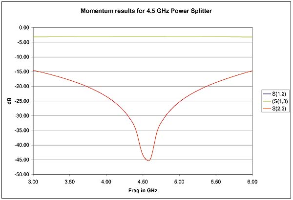
The throughput is S(1,2) and S(1,3), which lie on top of each other. All of the S parameters are symmetric, that is the indices can be swapped. Since the T-Junction is a broadband device, S(1,2) and S(1,3) are nearly flat at 3dB. The characteristic dip in S(2,3) comes from the departure of the 1/4-wave transformers away from the design frequency. The maximum of the dip was fine-tuned to be near the design frequency. The bandwidth of a power-splitter is nominally defined by S(2,3) ~ 20dB. For this splitter, the bandpass is about 3.5-5.5 GHz.
Broad Band
With many microwave devices, constructing a broadband version of a narrow-band version is just a matter of cascading sections. Such is the case for Wilkinson power splitters. The only rub is that each section must have 1/4-wave transformers of different characteristic impedance, and each resistor must be a different value. In practice, these values are arrived at by simulation. Li et al. have performed the arduous task and tabulated optimum parameters. They were able to build a very broadband splitter, from 2-18 GHz with 7 sections. Since we were not interested in such broad bandwidth, we could settle for the much smaller 3 section splitter. We used the values as listed in Li et al and verified them in simulation.
| Section | Impedance | Resistance |
|---|---|---|
| 1 | 57.485 | 400 Ohms |
| 2 | 70.71 | 211.46 |
| 3 | 86.98 | 107.18 |
Table 1 Values from Li et al. used to design broadband power splitter
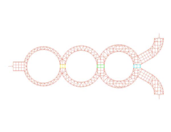
fig 4 Meshing of broad band power splitter. Each resistor is a different color to indicate the different resistivities of the material.
Each section of the power splitter is cut from a perfect ring, in keeping with the design in Li et al. Most of the filter was hand drawn, that is it was drawn using layout-only functions instead of transforming circuit elements. There is a gap of 25 mils cut in each section for the resistor to rest across. There were a few tweaks to the deign. The opening angle of the output transmission lines is not specified. We found out that smaller opening angle led to better S(1,2) and S(1,2), but to worse S(2,3). Obviously this was due to cross coupling between the outputs. Although the effect was not large, the angle used was a compromise.
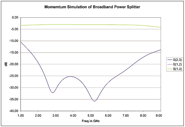
fig 5 Momentum results excel sheet pdf version
From the simulations we can see that S(2,3) shows the operating range of this device is between 2 and 7.5 GHz. In perfect circuit element simulation, there are 3 characteristic dips in S(2,3), the cross coupling. From Momentum, we see that there is a suppression of the 3rd dip around 7 GHz, presumably due to the failure of one of the circuit elements at high frequency. We also see that S(1,2) and S(1,3), the transmission, tapers at the ends of the band. This effect is not seen in the narrow band versions. Since the effect shows up far enough away from our operating frequencies, we did not worry about it.
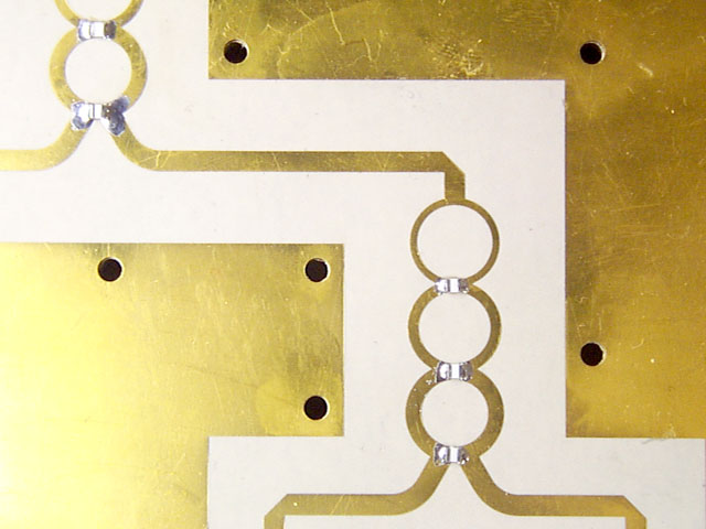
fig 6 Implementation of the design. Note how the resistors are "flip" mounted.